Chapter 10.1: 8086 Pins
Introduction
Learning Outcomes
Sort the 8086's 40 pins into groups; read active-low and active-high signals.
Explain how address and data share the same pins, and the role of ALE and the address latches.
Follow read and write cycles through T1–T4, with wait states (Tw), on a timing diagram.
Know minimum vs. maximum mode, the 8284A and 8288, and the interrupt pins (INTR, NMI, INTA').
Overview
The 8086 Package
- The Intel 8086 is a 16-bit HMOS microprocessor.
- It comes as a 40-pin DIP (dual in-line package) integrated circuit.
- Runs from a single +5 V DC supply (pin 40 = VCC, pins 1 and 20 = GND).
- A 20-line address bus (A0–A19) and a 16-line data bus (D0–D15).
- The address bus is multiplexed: one pin serves different purposes at different times.
- The 16 low address lines (A0–A15) are multiplexed with data → AD0–AD15.
- The 4 high address lines (A16–A19) are multiplexed with status → A16/S3 … A19/S6.
A signal whose name ends in ' (an overbar in the data sheet) is active low: it acts at 0 V. E.g. RD' = 0 → read.
In names like MN/MX', the MN meaning applies at 1 and MX at 0.
Direction: I = input, O = output, I/O = bidirectional.
Overview
Pin Diagram (Interactive)
Overview
Inside the Chip: Die Photo
- The silicon die sits in the middle of the package; bond pads along its edges are wired to the 40 pins.
- The AD bus pads on the left edge lead to the address/data pins.
- On the left: the 16-bit registers, the ALU and the prefetch queue; bottom right: the microcode ROM that executes instructions.
- About 29,000 transistors, 3 µm HMOS process.
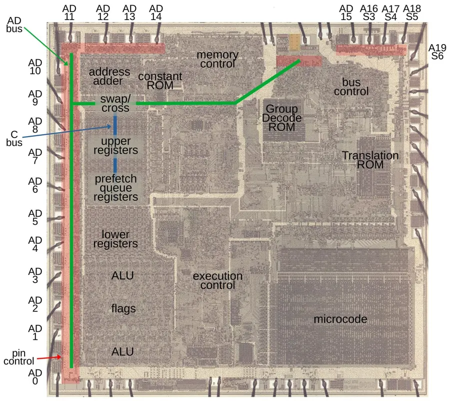
Photo: Ken Shirriff (righto.com), functional blocks marked.
Overview
Why Are the Pins So Complicated?
A microprocessor reaches memory and I/O through its data and address buses. On the 8086 this gets complicated for two reasons:
- 20 address + 16 data + ~20 control + power/clock: ≈ 60 signals.
- Solution: address, data and status share the same pins at different times (time-division multiplexing).
- The address formed with the segment registers is 20 bits; the data bus is only 16 bits.
- The extra 4 address bits (A16–A19) share their pins with status signals (S3–S6).
Overview
Pin Groups
| Group | Pins | Note |
|---|---|---|
| Power | VCC (40), GND (1, 20) | +5 V ± 10% |
| Clock and reset | CLK (19), RESET (21), READY (22) | from the 8284A clock generator |
| Address/data | AD0–AD15 (2–16, 39) | address in T1, then data |
| Address/status | A16/S3–A19/S6 (38–35), BHE'/S7 (34) | address in T1, then status |
| Interrupt | NMI (17), INTR (18), INTA' (24, min) | hardware interrupts |
| Common control | RD' (32), TEST' (23), MN/MX' (33) | same in both modes |
| Mode-dependent | 24–31 | min: INTA', ALE, DEN', DT/R', M/IO', WR', HLDA, HOLD max: QS1, QS0, S0', S1', S2', LOCK', RQ'/GT1', RQ'/GT0' |
Overview
Minimum and Maximum Mode
- MN/MX' = 1 (VCC) → minimum mode: a small single-processor system; the 8086 generates the control signals itself.
- MN/MX' = 0 (GND) → maximum mode: a multiprocessor or coprocessor (8087) system; the 8288 bus controller generates the control signals, and the freed pins carry status and bus arbitration.
- The mode is fixed in hardware by tying the pin; it never changes at run time.
| Pin | Minimum | Maximum |
|---|---|---|
| 24 | INTA' | QS1 |
| 25 | ALE | QS0 |
| 26 | DEN' | S0' |
| 27 | DT/R' | S1' |
| 28 | M/IO' | S2' |
| 29 | WR' | LOCK' |
| 30 | HLDA | RQ'/GT1' |
| 31 | HOLD | RQ'/GT0' |
Address and Data
Address/Data Bus Pins
- The low 16 address lines, multiplexed with data.
- Called A while carrying an address: A0–A15 (T1).
- Called D while carrying data: D0–D7, D8–D15 or D0–D15 (T2–T4).
- Bidirectional (output on writes, input on reads); floats (high impedance) when needed.
- The high 4 address lines, multiplexed with status signals.
- A16–A19 in T1 (on memory accesses), S3–S6 in T2–T4.
- Low during T1 of an I/O access (I/O addresses are 16 bits).
- S3, S4: which segment is in use; S5: the IF flag; S6: always 0.
Address and Data
Demultiplexing: ALE, Latches and Buffers
AD0–AD15 carry both address and data. The rest of the system needs separate, stable address and data buses.
T1: the 8086 puts the address on the AD pins and raises ALE. On ALE's falling edge the 8282 latch captures the address.
T2–T4: the same pins now carry data. DEN' = 0 enables the transceiver; DT/R' sets the direction (1: CPU → memory, 0: memory → CPU).
The latch holds the address steady for memory and I/O through the whole cycle. A16–A19/BHE' get a latch of their own (three 8282s in all).
Address and Data
A Buffered, Latched System
Buffers both demultiplex the bus and add drive strength: the 8086's pins can drive only a few loads, so large systems buffer every bus.
Address and Data
BHE' and A0: Memory Banks
| BHE' | A0 | Transfer |
|---|---|---|
| 0 | 0 | whole word, D0–D15 (even address) |
| 0 | 1 | high byte, D8–D15 (odd address) |
| 1 | 0 | low byte, D0–D7 (even address) |
| 1 | 1 | none |
Address and Data · Step through the code
Code Trace: Aligned and Unaligned Access
AX ← 2000h. Only instruction fetch cycles; no data access.
DS ← 2000h: the data segment starts at 20000h.
AX ← 1234h (AH=12h, AL=34h).
PA = 20100h is even: BHE'=0, A0=0 → both banks at once. The word is written in one cycle; AL to the even address (34h), AH to the odd one (12h).
AX ← ABCDh.
PA = 20101h is odd. Cycle 1: BHE'=0, A0=1 → high bank only. CDh from AL goes over D8–D15 to 20101h.
Cycle 2: PA = 20102h, BHE'=1, A0=0 → low bank only. ABh from AH goes over D0–D7. Unaligned word = 2 cycles.
Byte read, even address: BHE'=1, A0=0 → D0–D7. AL ← 34h, AH unchanged → AX = AB34h.
Unaligned word read. Cycle 1: CDh at 20101h arrives on D8–D15; the CPU steers it into BL.
Cycle 2: ABh at 20102h arrives on D0–D7 → BH. Result BX = ABCDh (little-endian).
mov ax, 2000h
mov ds, ax
mov ax, 1234h
mov [0100h], ax    ; even address
mov ax, 0ABCDh
mov [0101h], ax    ; odd address
mov al, [0100h]    ; byte
mov bx, [0101h]    ; odd address
Bus Cycles
Bus Cycles and T States
- Every data transfer between the CPU and memory or I/O is a bus cycle.
- A bus cycle takes at least four clock cycles: T1, T2, T3, T4 (the T states).
- Pin functions change with the T state: address in T1, data/status in T2–T4.
- For slow memory, wait states (Tw) are inserted between T3 and T4.
- Clock cycles in which the CPU leaves the bus unused are idle states (Ti).
T = 1 / 5 MHz = 200 ns
Bus cycle = 4 × 200 = 800 ns
At most 1 / 800 ns = 1.25 million bus cycles/s
2 bytes per word → ≈ 2.5 MB/s bus bandwidth
Bus Cycles
The Write Bus Cycle
A write cycle has four T states. Each T state starts at a falling clock edge.
T1: the target address goes out on the AD and A pins; ALE loads it into the external latches.
T2: the AD pins now carry the data to write; WR' goes to 0.
T3: data and WR' stay stable; memory captures the data (if READY = 0, Tw states go in here).
T4: WR' returns to 1 and memory completes the write on that rising edge; the bus gets ready for the next cycle.
In a write, the address is on the pins in T1 and the data in T2–T4 with no gap, because the CPU itself is the source of the data.
Bus Cycles
The Read Bus Cycle
A read cycle also has four T states, but on the AD pins there is a gap (float) between address and data.
T1: as in a write, the address goes out on the pins and is latched.
T2: the 8086 switches its AD output drivers to tri-state (high impedance) → memory can drive the bus. RD' = 0.
T3: memory (or the I/O device) puts the requested data on the bus.
T4: at the start of T4 the 8086 samples the data on its pins; RD' = 1, memory releases the bus.
The float in T2 is for bus turnaround: if memory started driving data before the CPU stopped driving the address, the two outputs would collide.
Bus Cycles
Read Cycle Timing
All control signals of a memory read cycle in minimum mode.
T1: M/IO' = 1 (memory), address on the pins; ALE pulse latches it; DT/R' = 0 (receive).
T2: AD floats, S6–S3 replace A19–A16; RD' = 0, then DEN' = 0 → transceiver enabled.
T3: memory drives the data. During T3 the CPU samples READY: if it is 1, the CPU moves on to T4.
T4: the data is sampled; RD', DEN', DT/R' go inactive; M/IO' may change for the next cycle.
Bus Cycles
READY and Wait States (Tw)
If slow memory cannot have its data ready by T3, it pulls READY low.
READY = 0 is seen in T3 → the CPU does not enter T4 but inserts a Tw (wait) state. All signals stay as they are.
READY is sampled again at the end of Tw; now it is 1 → memory is ready. More than one Tw can be inserted if needed.
T4: the data is read. The cycle took 5 × 200 = 1000 ns (one wait state = +200 ns).
READY reaches the 8086 from the 8284A's RDY input, synchronized to the clock (active high).
Bus Cycles
How Many Wait States?
- In a read, the address is valid at most TCLAV after T1 starts; data is sampled at the end of T3, on the clock edge into T4, and must be ready TDVCL before it.
- The address latch, address decoder and data transceiver delays (tbuf) also eat into that time.
- Each Tw stretches the window by one T.
Condition: tacc ≤ tallow + n·T → n = ⌈(tacc − tallow) / T⌉ (n = 0 if negative)
Since RD' falls in T2, the RD' → data time (output enable) adds a second condition; only the address → data condition is computed here.
T = 200 ns; data sheet: TCLAV ≤ 110 ns, TDVCL ≥ 30 ns; assume tbuf = 40 ns.
tallow = 600 − 110 − 30 − 40 = 420 ns
Memory tacc = 700 ns:
n = ⌈(700 − 420) / 200⌉ = ⌈1.4⌉ = 2 Tw
Check: 1 Tw → 620 ns < 700 ✗; 2 Tw → 820 ns ≥ 700 ✓
Cycle = (4 + 2) × 200 = 1200 ns
With tacc = 400 ns: 400 ≤ 420 → 0 Tw.
Status Pins
S2', S1', S0' Status Pins
- In maximum mode (pins 26–28) they encode the type of bus cycle.
- Active during T4 (of the previous cycle), T1 and T2.
- Return to the passive state (1, 1, 1) in T3, or in a Tw with READY = 1.
- The 8288 bus controller decodes them into memory and I/O control signals (MRDC', MWTC', IORC' …).
- A change from passive to any other code in T4 signals that a new bus cycle is starting.
Low signal = 0 ≈ 0 V
High signal = 1 ≈ +5 V
The status pins are active low, so “111 = passive” means “nothing happening”.
Status Pins
S2' S1' S0' Codes
| S2' | S1' | S0' | Cycle | 8288 command |
|---|---|---|---|---|
| 0 | 0 | 0 | Interrupt acknowledge | INTA' |
| 0 | 0 | 1 | Read I/O port | IORC' |
| 0 | 1 | 0 | Write I/O port | IOWC', AIOWC' |
| 0 | 1 | 1 | Halt (HLT) | none |
| 1 | 0 | 0 | Code access (instruction fetch) | MRDC' |
| 1 | 0 | 1 | Read memory | MRDC' |
| 1 | 1 | 0 | Write memory | MWTC', AMWC' |
| 1 | 1 | 1 | Passive | none |
S2' = 1 → memory, S2' = 0 → I/O / special.
S1' and S0': 01 → read, 10 → write.
That is why S2' shares a pin with minimum-mode M/IO', and S1' with DT/R'.
Status Pins
S3–S6 and BHE'/S7 Status Bits
A16/S3, A17/S4, A18/S5, A19/S6: status bits instead of address after T1.
| S4 (A17) | S3 (A16) | Segment in use |
|---|---|---|
| 0 | 0 | ES (extra segment) |
| 0 | 1 | SS (stack) |
| 1 | 0 | CS or no segment (I/O, interrupt vector) |
| 1 | 1 | DS (data) |
- S5 (A18): current value of the IF flag, updated at the start of every clock cycle.
- S6 (A19): always 0 (the 8086 owns the bus).
- S7 (BHE'): an unused spare status bit.
S3–S4 let a system attach a separate 1 MB of memory per segment (e.g. the stack in its own bank).
Status Pins · Step through the code
Code Trace: Instructions and Status Codes
org 100h
mov bx, 0200h
mov ax, [bx]      ; memory read
mov [bx+2], ax    ; memory write
in al, 60h        ; I/O read
out 61h, al       ; I/O write
push ax           ; stack write
hlt               ; halt
At the start of every cycle the 8086 puts the cycle type on S2' S1' S0'. mov bx, 0200h needs only a code fetch: 100; S4 S3 = 10 → CS.
mov ax, [bx]: memory read 101. The 8288 issues MRDC'. The data segment is used, so S4 S3 = 11 (DS). AX = 1234h.
mov [bx+2], ax: memory write 110 → 8288 MWTC' (and AMWC' one clock earlier). The segment is DS again.
in al, 60h: I/O read 001 → IORC'. I/O uses no segment: S4 S3 = 10. AL = 5Ah.
out 61h, al: I/O write 010 → IOWC'. With S2' = 0, memory stays out of this cycle.
push ax is a memory write too (110), but it uses the stack segment: S4 S3 = 01 (SS). A system could put the stack in a separate bank.
hlt: 011 is the halt code; the 8288 issues no command. Between cycles the pins return to 111 (passive).
The 100 (code fetch) cycles that fetch the instruction bytes come on top of these.
Status Pins
Demo: Status Code Decoder
Click a pin to toggle it between 0 and 1; below you see how the 8288 and the system read the code.
Status Pins
QS1, QS0: Queue Status
- In maximum mode (pins 24–25) they report the state of the prefetch queue.
- Valid in the clock cycle after the queue operation.
- The 8087 coprocessor uses them to follow which instruction the 8086 is executing and to catch its own (ESC) instructions.
| QS1 | QS0 | Status |
|---|---|---|
| 0 | 0 | No operation (queue unchanged) |
| 0 | 1 | First byte of an opcode taken from the queue |
| 1 | 0 | Queue emptied (branch) |
| 1 | 1 | Subsequent byte taken from the queue |
Control Pins
RD', WR' and M/IO'
- Output, active low.
- Signals that the CPU is reading from memory or I/O.
- 0 during T2, T3 and any Tw of a read cycle.
- Output, active low; 0 during T2, T3 and Tw of a write cycle.
- Tells memory and I/O accesses apart.
- 1 → memory operation (M active), 0 → I/O operation (IO' active).
- Valid from T4 of the previous cycle through the whole cycle.
- Inverted on the 8088: IO/M'.
| M/IO' | RD' | WR' | Operation | Example instruction |
|---|---|---|---|---|
| 1 | 0 | 1 | memory read | MOV AL, [BX] |
| 1 | 1 | 0 | memory write | MOV [BX], AL |
| 0 | 0 | 1 | I/O read | IN AL, 60h |
| 0 | 1 | 0 | I/O write | OUT 43h, AL |
Control Pins
DT/R' and DEN'
- Needed in systems with an 8286/8287 data bus transceiver.
- A transceiver is a transmitter and receiver in one package.
- 1 → data out of the CPU (write), 0 → into the CPU (read).
- It drives the transceiver's T input, which sets the data direction.
- Wired to the transceiver as output enable (OE').
- Active low during memory and I/O accesses and INTA cycles.
- Stays 1 in T1 so the address on the AD pins doesn't leak onto the data bus.
The correct name is DT/R': the R is active low.
Control Pins · Step through the code
From Instruction to Bus Cycles: OUT and IN
Cycle 1, T1: instruction bytes are read from memory. PA = 01A70h + 0018h = 01A88h (even) → BHE' = 0, A0 = 0: one word in one cycle. The ALE pulse latches the address; it is a read, so DT/R' = 0.
T2–T4: RD' = 0, DEN' = 0. Memory returns the word: E6h (opcode) from the even address on D7–D0, 59h (port) from the odd address on D15–D8.
Cycle 2, T1: M/IO' = 0 → I/O. Only A7–A0 carry the address (59h); A15–A8 and A19–A16 = 0. The port address is odd → BHE' = 0, A0 = 1. Write: DT/R' = 1.
T2–T4: WR' = 0. 12h from AL goes out on D15–D8 (odd address = high bank). The output port usually latches the data as WR' rises.
Cycle 3, T1: the next instruction is at 01A8Ah (even) → again one word fetch. M/IO' = 1, DT/R' = 0.
T2–T4: E4h (IN AL, imm8) is read on D7–D0, 9Ah (port) on D15–D8.
Cycle 4, T1: I/O address 009Ah is even → BHE' = 1, A0 = 0: low bank only. Read: DT/R' = 0.
T2–T4: RD' = 0; the port puts 3Ch on D7–D0, which enters AL at the start of T4. Bus activity: 4 cycles × 4 T = 16 clocks (no Tw).
; CS = 01A7h, AL = 12h
; PA      bytes  instr
01A88h  E6 59  out 59h, al
01A8Ah  E4 9A  in  al, 9Ah
A simplified sequential model: in reality the BIU prefetches code whenever the queue has room, so cycle 3 may come before cycle 2. T1–T4 details: Write and Read Bus Cycle. If an 8-bit device sits only on D7–D0, odd port addresses cannot be used.
Control Pins
HOLD / HLDA (Minimum Mode)
Another bus master (e.g. an 8237 DMA controller) wants the local bus.
HOLD = 1 (active high). The CPU finishes its current bus cycle.
In the middle of T4 or Ti, HLDA = 1 grants the request; the address, data and control pins float.
The DMA controller uses the bus. The 8086 can keep executing from its queue but waits as soon as it needs the bus.
HOLD = 0 → the CPU drops HLDA, takes the bus back and starts a new cycle.
Per the data sheet, HLDA is issued in the middle of T4 or of a Ti (idle) state.
Control Pins
RQ'/GT0', RQ'/GT1' and LOCK'
- Used by other local bus masters (e.g. the 8087).
- Forces the CPU to release the local bus at the end of a cycle.
- Each pin is bidirectional: a pulse sequence on one line → request (RQ), grant (GT), release.
- RQ'/GT0' has higher priority than RQ'/GT1'.
- The maximum-mode counterpart of HOLD/HLDA.
- Active-low output.
- While it is active, other bus masters are not allowed to take the system bus.
- Active throughout a
LOCK-prefixed instruction (until it completes). - For semaphores in multiprocessor systems:
LOCK XCHG AL, [BX]makes the read-modify-write atomic. - Also active automatically during INTA cycles.
Control Pins · Step through the code
Code Trace: Atomic Access with LOCK XCHG
org 100h
mov bx, offset flag
retry: mov al, 1
lock xchg al, [bx]   ; read + write
cmp al, 0            ; was it free?
jne retry            ; busy: retry
; ... critical section ...
mov byte ptr [bx], 0 ; release
ret
flag db 0
The shared memory flag (0110h) is a semaphore shared by two CPUs: 0 = free, 1 = busy. It is free now.
AL = 1: the “busy” value to store in the flag.
lock xchg starts: LOCK' = 0. Bus cycle 1 reads the flag (0). The other master's RQ/GT request is not granted meanwhile.
Bus cycle 2 writes the 1 from AL into the flag; AL got the old value (0). Between the read and the write, no other CPU could get in.
XCHG done, LOCK' = 1: the bus can be shared again. cmp al, 0: old value 0 → ZF = 1.
jne is not taken: the flag was free and is now ours. If the other CPU tries, xchg returns 1 to it and it keeps waiting.
Critical section done: writing flag = 0 releases the semaphore.
Without the LOCK prefix, the other CPU could grab the bus between the read and write cycles and read the same 0; both CPUs would enter the critical section.
Control Pins
TEST' and CLK
- Tested by the
WAITinstruction. - If TEST' = 0, execution continues; otherwise the CPU idles and tests the pin again.
- Synchronized internally on every rising clock edge.
- Typical use: wired to the 8087's BUSY output;
FWAITwaits for the 8087 to finish.
CLK (pin 19): the basic timing for the CPU and bus control. An asymmetric square wave with a 33% duty cycle.
8086: 5 MHz, 8086-2: 8 MHz, 8086-1: 10 MHz.
Control Pins
RESET, VCC and GND
- RESET (pin 21): stops whatever the CPU is doing immediately. It must stay 1 for at least four clock cycles (at least 50 µs at power-up). When it falls, the CPU restarts.
- VCC (pin 40): +5 V DC supply.
- GND (pins 1, 20): ground. Two ground pins reduce noise from high-current switching.
| After reset | Value |
|---|---|
| CS | FFFFh |
| IP | 0000h |
| DS, SS, ES | 0000h |
| FLAGS | cleared (IF = 0: interrupts off) |
| Queue | empty |
| First instruction at | FFFF0h + 0000h = FFFF0h |
JMP to the real startup code.Control Pins · Step through the code
What the CPU Does: RESET → First Instruction
; RESET = 1 (≥ 4 clocks)
CS ← FFFFh, IP ← 0000h
DS, SS, ES ← 0000h
FLAGS ← 0000h  ; IF = 0
flush the queue
; RESET 1 → 0
fetch FFFF0h   ; EA 5B E0 00 F0
jmp far F000h:E05Bh
fetch FE05Bh   ; BIOS
RESET is held at 1 for at least four clocks: the CPU drops what it is doing. Register contents are undefined.
The hardware loads CS = FFFFh, IP = 0000h. The programmer doesn't choose these values.
The other segment registers become 0000h.
Flags are cleared; IF = 0: interrupts are off, so the startup code runs uninterrupted.
The queue is empty. When RESET drops to 0, the BIU starts the first fetch.
First address: FFFFh × 10h + 0000h = FFFF0h, in the last 16 bytes of the 1 MB space. The ROM holds a 5-byte far jump here: EA 5B E0 00 F0.
EA = far JMP: offset first (E05Bh), then segment (F000h), both little-endian. CS:IP = F000h:E05Bh; the queue is flushed again.
New address F0000h + E05Bh = FE05Bh: the BIOS startup code (its IBM PC address). The startup code that doesn't fit in 16 bytes continues here.
Control Pins
8284A Clock Generator
- Divides the crystal frequency by 3: 15 MHz → 5 MHz CLK, 33% duty cycle.
- Synchronizes READY and RESET to the clock; a Schmitt trigger on RES' turns the slowly rising RC voltage into a clean RESET.
Control Pins
MN/MX' and Mode-Dependent Pins
- ALE (25): address latch enable; an active-high pulse in T1 that loads the 8282/8283 latches. ALE is never floated.
- INTA' (24): interrupt acknowledge.
- DEN', DT/R', M/IO', WR': transceiver and memory/I/O control.
- HOLD, HLDA: bus handover (DMA).
- S2', S1', S0': cycle type → the 8288 generates the control signals.
- QS1, QS0: queue status (for the 8087).
- LOCK': locks the bus.
- RQ'/GT0', RQ'/GT1': bus request/grant.
Data sheet: “ALE is never floated”, i.e. ALE never goes to high impedance.
Maximum Mode
8288 Bus Controller
- In maximum mode it decodes the 8086's S2'–S0' code.
- Commands: MRDC' memory read, MWTC' memory write, IORC'/IOWC' I/O read/write, INTA' interrupt acknowledge. The “A” versions (AMWC', AIOWC') are “advanced” write strobes that start one clock earlier.
- Control: ALE, DEN and DT/R' now come from the 8288 (DEN is active high here).
- The 8086 reuses the freed pins for QS, LOCK' and RQ'/GT'.
Maximum Mode
A Maximum-Mode 8086 System
The 8284A supplies the clock; the 8288 generates the commands and ALE/DEN/DT/R'; latches drive the address bus and transceivers the data bus; the 8259A interrupt controller feeds 8 hardware interrupts (IRQ0–7) into INTR.
Interrupts
INTR, NMI and INTA'
- Level-triggered, active-high input.
- Sampled in the last clock cycle of each instruction.
- Accepted if IF = 1 (maskable: CLI disables it).
- When it is accepted, the CPU runs interrupt acknowledge cycles.
- Synchronized internally.
- Edge-triggered (0 → 1 transition).
- Always causes a type 2 interrupt; the routine in the vector table runs.
- Cannot be masked by software (IF).
- Taken at the end of the current instruction.
- Uses: power failure, memory parity error.
- Active-low output.
- 0 during T2, T3 and Tw of the acknowledge cycle.
- Two back-to-back INTA' pulses; on the second, the interrupt controller puts the type number on D0–D7.
- In max. mode the 8288 generates it.
INTR is level-triggered; NMI is the edge-triggered one.
Interrupts
Hardware Interrupts: INTA Cycles
INTR = 1 and IF = 1 → when the current instruction ends, the CPU runs two interrupt acknowledge cycles.
First INTA' pulse: tells the interrupt controller (8259A) “your request is accepted”. The data bus stays floating.
Second INTA' pulse: the 8259A puts the interrupt type number (e.g. IRQ0 → 08h) on D7–D0; the CPU reads it.
In max. mode, LOCK' is active from T2 of the first cycle to T2 of the second, so no other master can take the bus in between.
Summary
Summary
AD0–AD15: address in T1, then data; A16–A19: address in T1, then S3–S6. ALE + 8282 latches hold the address.
T1 address, T2 direction/command, T3 data, T4 finish. READY = 0 → Tw. 800 ns at 5 MHz.
Even/odd bank select. An unaligned word takes two cycles.
MN/MX' = 1: the 8086 generates the control signals. 0: S2'–S0' → 8288.
8284A: 15 MHz / 3 = 5 MHz, 33% duty; after RESET, FFFF:0000h.
INTR: level, masked by IF; NMI: edge, type 2. Acknowledge takes two INTA' pulses; the type number is on D7–D0 in the second.
Summary
Exercises
- An 8086 runs at 8 MHz. How many ns does a bus cycle take with no wait states? With two Tw?
- What values do M/IO', RD', WR' and DT/R' take while writing to a peripheral (OUT)?
- How many bus cycles does
MOV [2003h], AXneed? What are BHE' and A0 in each? - What is the difference between S2' S1' S0' = 1 0 0 and 1 0 1? Which command does the 8288 issue for each?
- The 8259A reports IRQ0 as type 08h. What is on the data bus during the two INTA' pulses? What is LOCK' doing meanwhile in maximum mode?
- With a 24 MHz crystal, what CLK does the 8284A produce? Which 8086 version suits it?
Hints / answers
- T = 125 ns → 4 × 125 = 500 ns; with two Tw, 6 × 125 = 750 ns.
- M/IO' = 0, RD' = 1, WR' = 0, DT/R' = 1 (out of the CPU).
- Odd address → 2 cycles: 2003h (BHE'=0, A0=1, AL → D8–D15), 2004h (BHE'=1, A0=0, AH → D0–D7).
- 100 is a code (instruction) fetch, 101 a data read; both give MRDC'. The difference matters to observers such as the 8087.
- Pulse 1: the data bus floats (acknowledge only); pulse 2: the 8259A puts 08h on D7–D0. LOCK' stays 0 (active) from T2 of the first cycle to T2 of the second.
- 24 / 3 = 8 MHz → 8086-2.
Summary
Exercises (2)
- With T = 125 ns and TCLAV + TDVCL + tbuf = 120 ns, how many Tw does a memory with 450 ns access time need?
- In the I/O write cycle of
OUT 9Bh, AL, what are A7–A0, BHE' and A0, and which lines carry the data?
Hints / answers
- tallow = 375 − 120 = 255 ns; ⌈(450 − 255) / 125⌉ = ⌈1.56⌉ = 2 Tw (1 Tw: 380 ns is too short, 2 Tw: 505 ns is enough); cycle 6 × 125 = 750 ns.
- A7–A0 = 9Bh (A19–A8 = 0), M/IO' = 0; odd address → BHE' = 0, A0 = 1; AL goes out on D15–D8.
Summary
References
- Intel, 8086 16-Bit HMOS Microprocessor data sheet (231455).
- Intel, 8284A Clock Generator and Driver, 8288 Bus Controller, 8282/8283 Octal Latch data sheets.
- B. B. Brey, The Intel Microprocessors, 8th ed., Pearson, 2009 (Chapter 9: 8086/8088 hardware specifications).
- D. V. Hall, Microprocessors and Interfacing, 2nd ed., McGraw-Hill.
- M. Bodur, Mikroişlemcilere Giriş: Assembler ile Yazılım ve Arayüz, EMO, 2014 (in Turkish).
- K. Shirriff, 8086 die photos and reverse-engineering articles, righto.com.